Fenix – USA
389 Palm Coast Parkway SW
Palm Coast, FL 32137
(803) 649-1381
info@fenix-mfg.com
Fenix – DR
San Pedro Industrial Free Zone
San Pedro De Macoris, Dominican Republic
(809) 529-4421
info@fenix-mfg.com
Fenix – USA
389 Palm Coast Parkway SW
Palm Coast, FL 32137
(803) 649-1381
info@fenix-mfg.com
Fenix – DR
San Pedro Industrial Free Zone
San Pedro De Macoris, Dominican Republic
(809) 529-4421
info@fenix-mfg.com
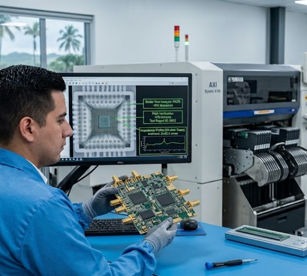
The manufacturing requirements for Radio Access Network (RAN) and 6G hardware demand extreme precision in Surface Mount Technology (SMT) to maintain high-frequency signal integrity. Production mandates strict thermal profiling for low-loss laminates, advanced void-reduction soldering for impedance control, and comprehensive 3D Automated Optical Inspection (AOI) paired with Automated X-Ray Inspection (AXI) to guarantee flawless multi-layer PCB assemblies.
As North American telecom providers aggressively build out the physical infrastructure for next-generation networks, the engineering tolerances for base stations, edge computing routers, and RAN hardware are shrinking. As networks push into higher mid-bands (7 GHz to 15 GHz) and sub-THz ranges for 5G-Advanced and early 6G, even microscopic manufacturing defects can cause catastrophic signal loss. To secure this critical infrastructure, telecom OEMs are shifting away from distant offshore suppliers and nearshoring telecom PCB assembly to highly regulated facilities closer to home.
The foundation of modern RAN hardware relies on flawlessly executed Surface Mount Technology (SMT). High-frequency boards require strict impedance control to prevent signal reflections and crosstalk at gigahertz frequencies.
To ensure reliable performance in PCB Assembly for telecom infrastructure, traditional visual inspections are entirely inadequate.
Quality control must be automated and deeply integrated into the assembly line.
For North American telecommunications companies, protecting proprietary RAN hardware designs is a matter of critical infrastructure security. By nearshoring production to the DR-CAFTA region, OEMs achieve synchronous EST communication and protect sensitive intellectual property within a secure legal framework, completely bypassing volatile trans-Pacific shipping lanes.
Why is impedance control critical in 5G-Advanced and 6G PCB assembly?
At gigahertz frequencies, any variation in the PCB’s physical structure or solder joints can alter the electrical impedance. This leads to signal reflections, crosstalk, and data loss, making strict impedance control mandatory during the SMT process.
Why are specialized low-loss laminates required for telecom PCBs?
Standard PCB materials can absorb and degrade high-frequency signals. Low-loss laminates are essential for maintaining signal integrity and thermal stability in RF, microwave, and modern RAN hardware applications, ensuring data is transmitted without distortion.
How does Automated X-Ray Inspection (AXI) benefit telecom hardware?
Telecom routers and base stations rely on dense microprocessors. AXI allows quality assurance engineers to see through components like Ball Grid Arrays (BGAs) to verify the structural and electrical integrity of hidden solder joints before deployment.
Explore Our Capabilities: