The Semiconductor Safety Valve: Securing Legacy Chip ATP and Packaging in the DR

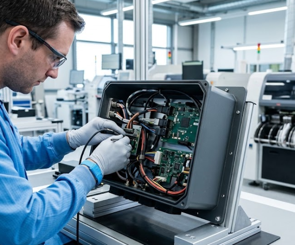
Electronics manufacturing technician assembling a complex electromechanical industrial box build enclosure at a nearshore EMS facility.

While global headlines focus on multi-billion-dollar wafer fabs for cutting-edge nanometer nodes, the global industrial, automotive, and medical infrastructure runs on mature nodes.

Legacy chip contract manufacturing—encompassing mature-node microcontrollers, power management ICs, analog sensors, and discrete components—remains the backbone of modern electronics.

However, wafer fabrication is only half the battle. Downstream Assembly, Test, and Packaging (ATP) has emerged as the critical bottleneck in the semiconductor supply chain.

With over 75% of global ATP capacity concentrated in East Asia, U.S. Original Equipment Manufacturers (OEMs) face persistent exposure to trans-Pacific shipping delays, geopolitical friction, and unexpected tariff shifts.

Establishing a nearshore ATP safety valve under the DR-CAFTA framework provides North American OEMs with the geographic, financial, and technical resilience required to hedge against trans-Pacific disruptions.

The ATP Bottleneck: Why Wafer Supply Is Not Enough

An unpackaged, untested silicon wafer cannot power an engine control unit or a medical device. Transforming raw wafers into production-ready integrated circuits requires precision back-end processing:

Back-End Production Workflow:

  • Raw Silicon Wafer → Precision Dicing & Etching → Die Attach & Wire Bonding → Encapsulation & EOL Testing →         2-Day Transit to US

Relying on distant back-end facilities introduces operational friction that compromises time-to-market:

  • Extended Freight Lead Times: Ocean transport of finished IC packages from Asia takes 30 to 45 days, exposing inventories to sea-freight volatility.
  • Capital Lock-Up: Prolonged logistics cycles tie up significant working capital in transit inventory.
  • Engineering Displacement: Managing engineering change orders (ECOs) or yield anomalies across a 12-hour time-zone gap delays root-cause resolution.

By shifting mature-node ATP and back-end processing to an EST-aligned nearshore contract manufacturer, fabless semiconductor companies and OEMs drastically compress the time between wafer fabrication and final product assembly.

Advanced Back-End Processing: Plasma Etching and Precision Assembly

Nearshore semiconductor packaging demands state-of-the-art material science and surface preparation to ensure high-reliability performance in demanding environments.

Reactive Ion Etching (RIE) and Inductively Coupled Plasma (ICP)

Prior to encapsulation and die attach, wafer surface preparation is vital for stress relief, surface activation, and contamination removal. Advanced nearshore facilities utilize:

  • Reactive Ion Etching (RIE): Chemical-physical dry etching that precisely removes surface layers and residue at the microscopic level without damaging sensitive active areas.
  • Inductively Coupled Plasma (ICP): High-density plasma processing that enables high-aspect-ratio etching and ultra-clean surface activation, ensuring superior adhesion during die attach and wire bonding.

These dry etching techniques eliminate micro-fractures during wafer dicing and prevent delamination in high-stress thermal cycling environments.

High-Density Packaging and Final Testing

Modern legacy chip packaging goes beyond simple plastic DIP or SOIC housings. Nearshore ATP integration encompasses:

  1. Precision Wafer Dicing & Thinning: Reducing die thickness while maintaining structural integrity.
  2. Advanced Wire Bonding: Gold, aluminum, and copper wire bonding for high-density pinouts.
  3. Conformal Encapsulation: High-purity epoxy molding compounds that shield the die from thermal, chemical, and mechanical shock.
  4. Automated Final Test (AFT): Wafer-level and package-level testing (parametric, functional, and burn-in) to deliver 100% verified, zero-defect ICs.

DR-CAFTA: Tariff Shields and 2-Day Logistics for Semiconductor Supply Chains

For U.S. semiconductor buyers, location determines total cost of ownership (TCO). Nearshoring back-end semiconductor ATP nearshoring to the Dominican Republic under DR-CAFTA provides structural advantages over traditional Asian packaging hubs.

Supply Chain Metric

Asian ATP Corridors

Fenix Nearshore ATP (DR-CAFTA)

Import Duties & Tariffs

Subject to Section 301 tariffs & policy shifts

0% Duty-Free Import Protection

Transit Time to U.S. Ports

30 to 45 Days (Ocean Freight)

2-Day Direct Ocean Shipping

Engineering Collaboration

12 to 14 hour time-zone gap

Real-time, same-timezone alignment (EST)

IP & Trade Protection

Complex multi-jurisdictional IP risk

Strong bilateral intellectual property protection

By locating legacy chip packaging within an EST-aligned hub, engineering teams can conduct real-time yield optimization and rapid failure analysis, ensuring uninterrupted production schedules.

De-Risk Your Back-End Semiconductor Supply Chain with Fenix

As global semiconductor demand accelerates, securing flexible, high-reliability back-end packaging close to home is no longer optional—it is a competitive necessity.

Fenix provides robust semiconductor ATP nearshoring capabilities, from advanced plasma etching (RIE/ICP) to high-precision assembly and automated final testing for critical sectors. Backed by DR-CAFTA tariff protection and direct 2-day delivery to major U.S. ports, Fenix is your strategic partner for complete supply chain resilience.

Ready to secure your legacy chip supply chain?

Contact our engineering team today to review your ATP specifications or explore our turnkey manufacturing solutions across specialized industries.

Frequently Asked Questions (FAQ)

What is semiconductor ATP, and why is nearshoring it critical?

ATP stands for Assembly, Test, and Packaging—the final back-end phase of semiconductor manufacturing where raw silicon wafers are diced, bonded, encapsulated into protective housings, and tested. Nearshoring ATP eliminates the multi-week trans-Pacific transit bottleneck between wafer fabs and final board assembly.

What role do RIE and ICP plasma etching play in semiconductor packaging?

Reactive Ion Etching (RIE) and Inductively Coupled Plasma (ICP) are dry etching processes used to clean, etch, and activate wafer surfaces at microscopic levels. They ensure proper stress relief and pristine surface adhesion before die attach and wire bonding, preventing field failures in harsh operating environments.

How does DR-CAFTA impact semiconductor packaging costs?

Under DR-CAFTA, qualifying semiconductor packages and integrated circuits assembled in the Dominican Republic enter the U.S. duty-free (0% tariff). This shields OEMs from shifting international tariffs while reducing freight expenses and working capital lock-up.
en_USEN